
3 Hot Electron Microscopy Applications for the Next Decade and Beyond
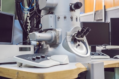
Electron microscopy has long been a staple microscopy technology, especially for characterization in the semiconductor industry as well as for other materials. However, new technological innovations combined with emerging industries have opened the door to new applications where electron microscopy is likely to be of significant demand for the long-term. According to SDi’s recent The 2019 Market for Electron Microscopy report, the electron microscopy market will grow 6% over the next five years and reach over $3.3 billion by 2023. Here are 3 hot applications where electron microscopy demand is projected to increase:
- Structural Biology
Historically, there have been many challenges with imaging biological samples via electron microscopy due to the harsh conditions a sample must endure. High vacuum sample chamber environments, the requirement for conductive samples, and the bombardment of electrons on a sample have long been considered serious limitations for biology research.
Today however, structural biology is relying more and more on electron microscopy to continue new discoveries and advancements. Cryo electron microscopy, in particular, is especially well-suited for bioimaging due to much less destructive sample conditions. In cryo-EM samples are essentially frozen in a specialized way in order to preserve the natural state of the biosample. In addition, other innovations such as lower vacuum requirements and advances in image processing software have optimized conditions for structural biology applications. The key is that electron microscopy and cryo-EM are bound to become even better adapted for structural biology applications as the technology develops. This will be significant because biosamples, which traditionally were only able to be characterized using light or fluorescence microscopy, can now be viewed at much higher magnification than ever before, opening the door to new insights and discoveries.
- Nanotechnology
Nanotechnology-based advances will be observed in virtually every industry over the next decade. From cancer therapeutics, to implant coatings that improve biocompatibility, to “smart” materials that adapt to their environment, nanotech products are likely to only accelerate in diversity and application. Nanotech and electron microscopy will go hand-in-hand due to the need to see and characterize smaller and smaller features. Tabletop electron microscopy systems enable the technology to be more accessible to end users via reduced price points. It is likely that more and more industries that did not traditionally need such magnification will require electron microscopy characterization due to the rapid emergence of nanotechnology-based products.
- MEMS
MEMS refers to microelectromechanical systems, which are basically electronic and/or mechanical systems that are submillimeter in scale. MEMS are manufactured using the same techniques long employed by the semiconductor industry yet they have much different applications and end markets. One of the most commercially successful examples of MEMS are airbag sensors which exist in automobiles. However, MEMS are becoming even more diverse such as in the form of microfluidic platforms for point-of-care diagnostics, advanced LED-chip displays, and even in micro-robotic surgery systems. Like semiconductors, MEMS will definitely demand high electron microscopy use for characterization throughout development and production.


